Microwave Engineering II
Lecture 9, 10 and 11: Oscillators
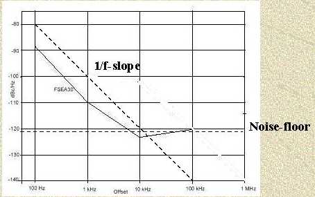
The oscillator is one of the most important RF-component together with the antenna, mixer and the amplifier for a modern receiver in a telecommunication system. Like we demand a low noise figure for the first amplifier in a system we also demand what is called low phase noise for the oscillator. In the section on noise we mentioned a type of noise called Flicker noise which has a 1/f dependence as a function of frequency, and is thus mostly pronounced for low frequencies. This noise will be up-converted and will display itself as a 1/f-noise sloop around the oscillation frequency, see Figures below. From the last figure you can easily image that if we have a close separation between the carriers as we have in a modern digital telecommunication system we will also easily have interference between the channels due to the phase noise.
1/f noise in dB below the carrier/Hertz (dBc/Hz) as a function of the distance (offset) from the carrier for an oscillator "FSC30".
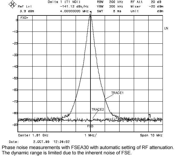
Up-converted 1/f-noise becomes the TRACE1 of the oscillator and is called phase-noise.
We will analyze how an oscillator starts to oscillate (deliver radio frequency power) and how we achieve a steady oscillation, i.e. what are the circuit requirements. (This lecture is probably the most abstract in the course).
Imagine that we have an amplifier where we feedback the signal from the output to the input in such a phase the the feed-backed signal will increase the output signal for the transistor. We can then easily imagine the case that after a short time the amplifier will be generating its own output independent of the input signal that we apply, see Figure below. Thus we will end up having an oscillator.
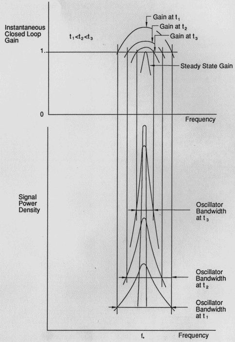
Figure showing the growth of the output signal. Notice how the signal "Signal Power Density" grows with time and becomes more narrow due to the interacting between the circuit in the amplifier and the active device (transistor). At the same time the gain of transistor reduces until it is equal to one. We then have a steady state oscillation.
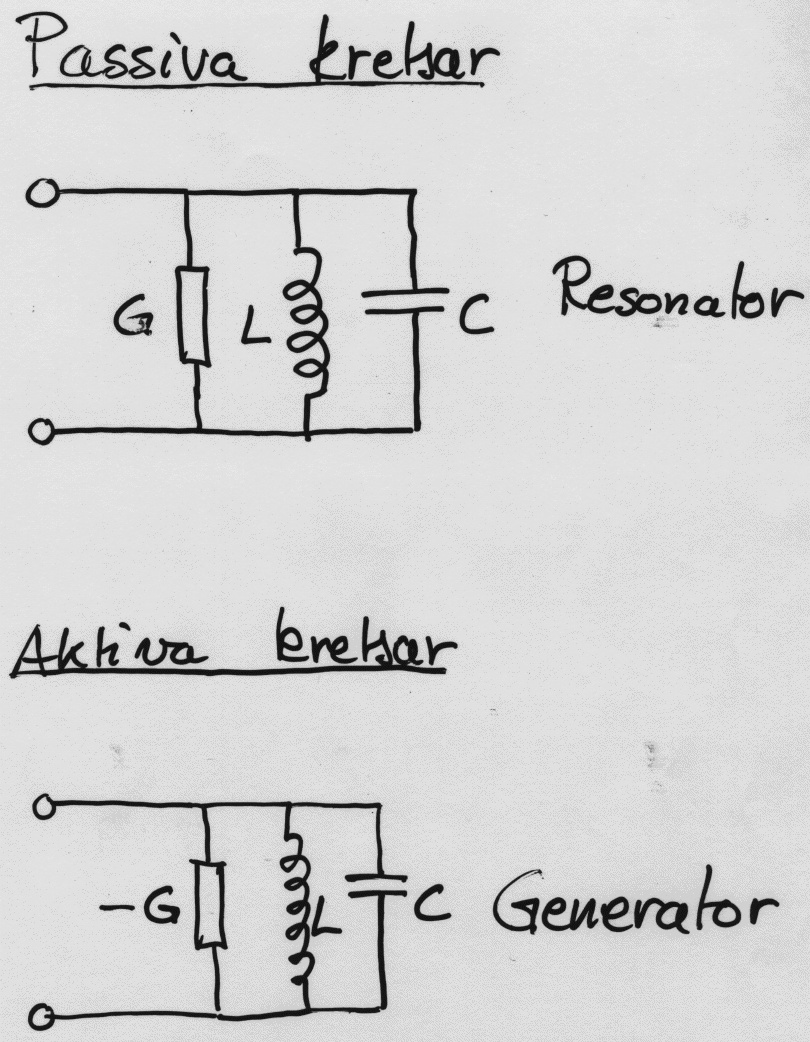
The oscillator is in principle a component that converts the DC-power to a RF-signal. We can create an oscillator by replacing the positive conductance (which absorbs power) in a passive parallel network with a negative conductance (which creates power).
As stated above the external circuit will have a strong influence on the level of the phase noise, see equation 11.85 in Pozar. We will discuss how the external circuit can be designed in order to both sustain the oscillation and suppress the phase noise.
Oscillator design
When we now have studied the reasons behind the phase-noise and what demands that we put on the external circuit we will start design oscillators. The oscillators can have a low phase-noise depending on the design of the outer circuit.
Single-port oscillator designs
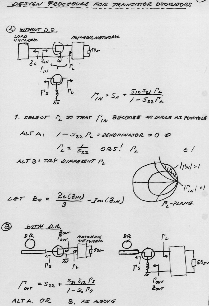
The first type of oscillator that we will design is the single port oscillator, i.e. the active component has only two terminals (e.g. a resonant tunneling diode). To sustain the oscillation we have to load the negative resistance component so that the oscillation can increase in strength and end with a steady state oscillation. As a role of thumb we load the device with an impedance whose real part is 1/3 of the absolute value of the negative resistance of the diode. In order for the oscillation to occur at the right frequency the reactive part of the load impedance has to be the conjugate of the device reactance. These role of thumbs is general for all oscillator designs, which means that we will use them also for the two-port oscillator design, see below..
Two-port oscillator designs
The two-port oscillators of the Non-Radiative Dielectric (NRD) and without NRD are designed around a transistor, where in the common emitter configuration the base - emitter is the input port and the collector - emitter will the output port (i.e. the port where we extract the power from the oscillator).
The design procedure for an oscillator without NRD can in simple terms be described using the following steps (see also figures below):
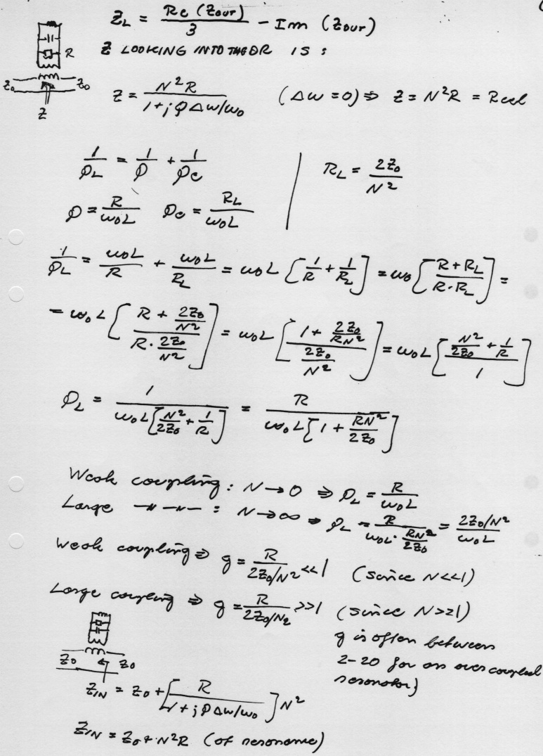
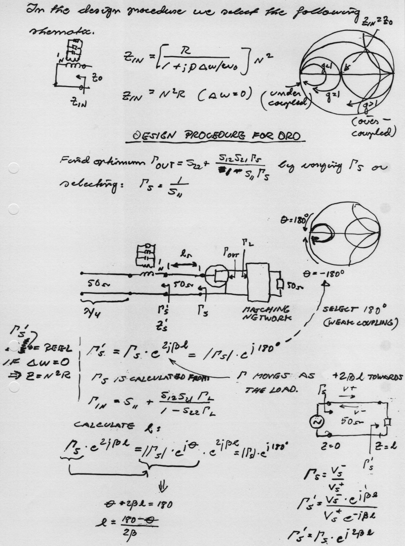
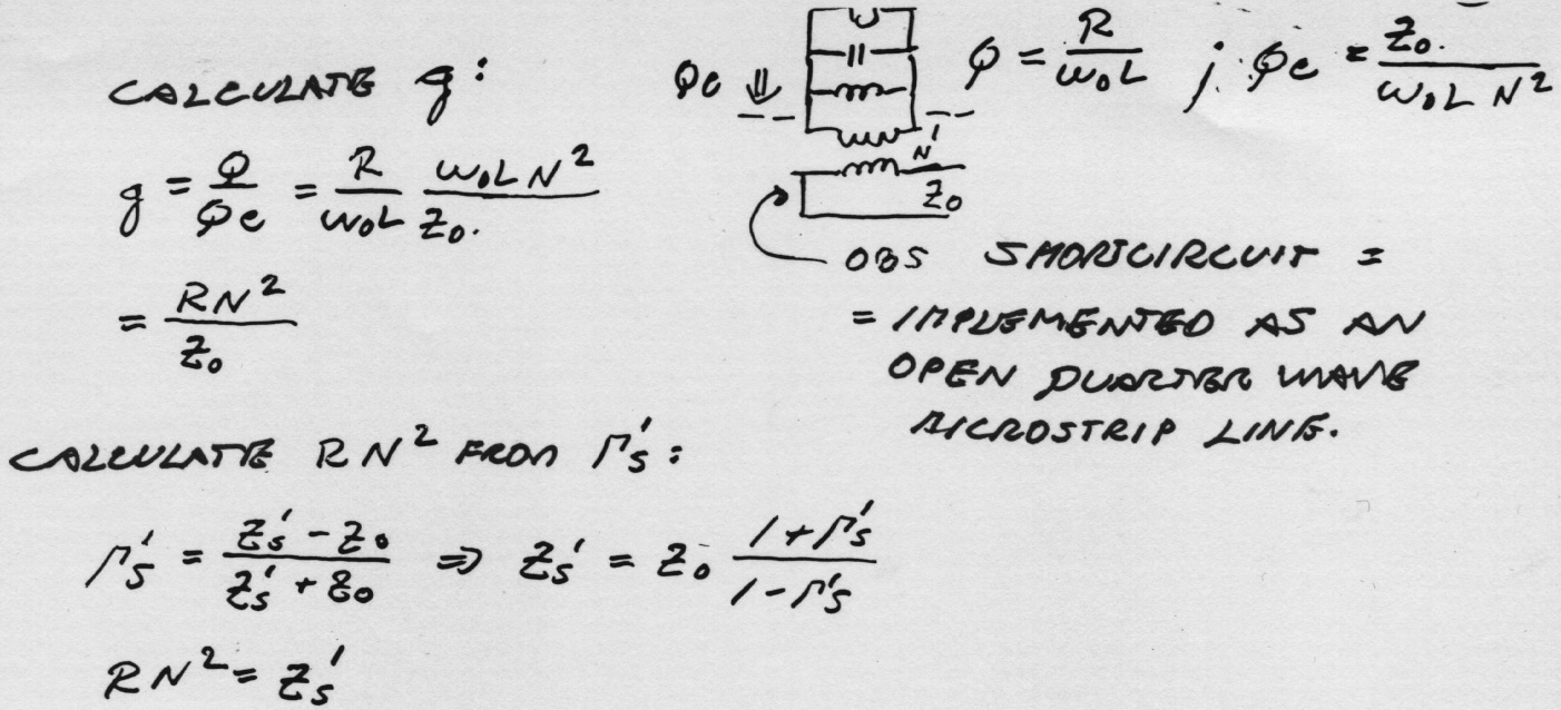
The design procedure for the NRD-oscillator is shown below. We assume that the NRD is under coupled which means that the maximum real impedance for the NRD will never become larger than Zo. The main steps in the design are:
To study:
Textbook pages: 641-652.
Below you find a recapitulation of the design procedure for transistor oscillators which we will go through in the lectures.
Important to understand:
Important equations: